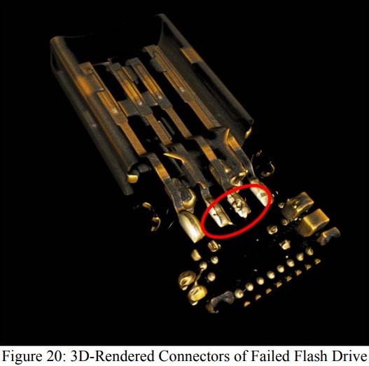
The industry is going through a transition in material sets for second level interconnects including adoption of leadfree solders. High-rel systems may often have a mix of components with different solder alloys in the printed circuit assemblies including both leaded and leadfree solders because some original leaded components may only be available in leadfree configurations. In this paper, the potential of x-ray micro-computed tomography (μCT) to fulfill the need for non-destructive three dimensional imaging of electronic assemblies has been evaluated. A number of defect seeded assemblies have been used for detection of a number of common solder interconnect defects and failure modes. In addition, the ability of the x-ray μCT for examination of complete products has been examined. Three-dimensional rendered versions of the board assemblies have been constructed for visualization of the defects and failure modes. Void sizes have been measured using Volume Graphics reconstruction and Matlab modules. In each case, the assemblies have been cross-sectioned after imaging by x-ray μCT to ascertain the morphology of the defect or failure mode using optical imaging. Results indicate that x-ray μCT is capable of providing high resolution imaging of the common defect types and failure modes in electronic assemblies and has potential for risk mitigation in sustainment of long-life high-rel systems.